Pinshine Laser Chemical Surface (PSLCS)
Process technical description
The size and performance trends of the next generation of electronic products require manufacturing technology to maximize space and reduce weight while providing more functions.
Molded interconnect devices (MID) and
Pin shine
Laser
Chemical
Surface molding technology (PSLCS) work together to integrate functions into a three-dimensional package, resulting in compact and lightweight high-performance devices.
Pin Shine Industrial Co., Ltd. was based on the 3D-MID conceptual design and develops a set of non-LDS process technology. It was referred to the requirement of making product housing mechanism on injection molding with general commercially available conventional plastics (non-LDS designated materials), and the product functionality is no longer limited to the characteristics of raw materials.
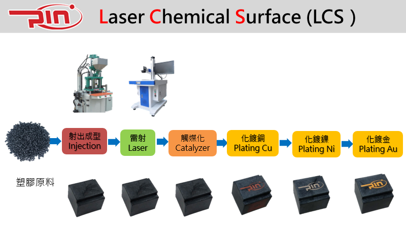
Above description, the laser machine with general standard specifications (non-LPKF special machine) was used in combination with the laser chemical surface molding technology (PSLCS) in the electroless plating process to generate metal wiring (layout) like PCB and form three-dimensional circuit board, which makes full use of all the space on the product surface and has penetration, which saves more space, makes the process simpler and the product more miniaturized.
The manufacturing process has the advantages of simple manufacturing process, easy assembly, reducing the number of workpieces and good integration: for example, the antenna element was integrated into the PCB element circuit.
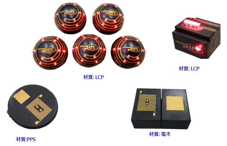
Material production:
- PC
- ABS
- PC/ABS
- PC+GF
- PTFE
- LCP
- PPA
- PS
- PPS
- PET&PBT
- Pl
- PPO
- PEEK
- PEI
- EPOXY
- Phenolic
PSLCS Process steps
- Injection Molding
- Laser Activated Chemical Surfaces
- Metalization
Applications:
All kinds of antennas(2G,3G,4G,5G,Wifi,NFC) ,Stereo Antenna, Sensor,AR/VR Wearable device, safety protection, earphone, simple circuit